The dicing process is a crucial step in semiconductor manufacturing. Choosing the right dicing method can impact the quality and yield of the final device.
Advanced laser dicing systems incorporate dynamic beam shaping technology to optimize the laser’s power, pulse duration, and focusing characteristics for specific material properties. This allows manufacturers to achieve high precision and accuracy while minimizing contamination risks.
Efficiency
The efficiency of laser dicing technology depends on several factors, including the type of laser used, the optical system, and the wafer material. For example, using a higher-powered laser source can increase the cutting speed and reduce kerf loss. However, this can also lead to higher temperatures and damage the wafer material. Therefore, it is important to select a laser with the right power level for each application.
The optical system is responsible for directing and shaping the laser beam to optimize cutting performance. This includes components such as mirrors, lenses, and beam expanders. Optimal optical systems can increase throughput and reduce waste while maintaining the quality of the diced dies. In addition, incorporating cleaning steps into the dicing process can further minimize contamination risks.
Plasma dicing uses a non-contact method, which can help reduce the mechanical stress on the wafers and chips. This can reduce the risk of chipping, cracking, or deformation, which is often a concern with traditional blade dicing. It is especially useful for fragile or stress-sensitive materials, such as silicon carbide, and advanced semiconductor devices with complex or delicate features.
Precision
The quality and precision of the separated chips in a wafer can have a significant impact on the performance of electronic devices that incorporate them. Therefore, it is critical that the dicing process is performed with the highest levels of accuracy and cleanliness. One of the most effective methods to achieve this is by using laser dicing technology. In addition, high-quality motion control systems can help ensure that the laser beam is precisely directed at the desired location on the workpiece.
Various types of lasers are used in dicing technology, including CO2, Nd:YAG, and ultra-short pulse lasers such as femtosecond and picosecond lasers. The type of laser that is selected depends on the material and application requirements. For example, a femtosecond laser can be more effective for cutting hard materials such as silicon or sapphire.
Moreover, the use of advanced control algorithms can improve dicing performance and ensure the quality of the diced wafers. This includes closed-loop feedback systems that monitor the dicing process in real-time and make adjustments accordingly. Additionally, integrating inspection and metrology tools can help verify the quality of the diced wafers.
Safety
Laser de-icing is a new non-contact and portable method for removing the ice adhering to high voltage transmission lines. This technology can effectively eliminate the ice, which threatens the safety and reliability of the power system. It also reduces the cost of glycol-based de-icing methods and avoids unnecessary damage.
Moreover, this technology is much safer than traditional cutting techniques. While laser dicing uses a lot of heat, it affects only a small area of the material being cut. This means that the materials will not warp or become damaged. It is also more precise than other types of cutting tools, and the laser does not require any wear or tear.
It is important to note that although this technology is very safe, it is still not suitable for all applications. Using lasers to cut some materials can cause damage, and evaporation of some substances can lead to toxic gases. Therefore, it is important to use this technique only in a controlled environment. This is especially important for semiconductor device fabrication, where the use of lasers has increased rapidly.
Accuracy
Laser cutting is a highly precise method for creating prototypes. The laser cuts so quickly that the material doesn’t have time to warp from excessive heat. Moreover, the heat is directed only where it is needed to cut or engrave, so there is very little damage to the surrounding area.
This accuracy is made possible by a CAD / CAM program that interprets the exact measurements of the design, sending them to the machine. This allows the machine to operate without requiring any human oversight, which saves time and money. Laser cutters can also be programmed to cut or engrave at a specific speed, which makes them more efficient than traditional machines that require manual supervision.
The results of the analysis are presented in Table 3. It can be seen that, in accordance with the expected results, laser processing visibly increases roughness parameters. Ra values of unprocessed reference samples are quite low, while Rz values are higher, ranging from 2.46 +- 0.17 to 8.90 +- 0.57 mm.
Flexibility
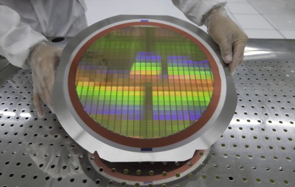
The semiconductor industry has experienced numerous innovations in wafer dicing systems, aimed at improving precision and accuracy while minimizing damage. One of these innovations is laser dicing, which offers several advantages over traditional blade dicing methods.
Laser dicing is non-contact, making it ideal for fragile or thin wafers. It also allows for a wide range of cut patterns, allowing manufacturers to precisely separate dies from one another. In addition, it is easy to integrate inspection and metrology tools into the dicing process, enabling manufacturers to monitor the quality of diced dies and identify any deviations from desired specifications.
Advanced laser dicing technology includes dynamic beam shaping, which allows manufacturers to adjust the shape and intensity of the laser beam according to material type and dicing needs. This flexibility reduces the risk of thermal damage and improves wafer dicing performance. For example, laser full cut dicing can achieve street width reductions of up to 96 % compared to blade dicing. This enables manufacturers to produce more chips from the same wafer and increase yield.
Cost
As the demand for advanced microelectronics grows, manufacturers face increasing pressure to improve yield and quality while reducing costs. One way to achieve these goals is to adopt laser dicing technologies. These cutting methods are non-contact, eliminating the stress that is associated with mechanical sawing and minimizing the risk of chipping and cracking. They also offer higher precision and narrower kerf widths, which allow chipmakers to pack more die on each wafer.
The key to laser dicing is the optic system, which directs and shapes the laser beam to deliver optimal performance. The optical system typically consists of mirrors, lenses, and beam expanders that work together to focus the laser energy on the surface of the wafer being cut. The design and quality of the optical system play a crucial role in ensuring that the dicing process is precise, efficient, and safe.
Thanks for visiting qasautos